SNSPD Research
Superconducting nanowires are capable of detecting a single photon when subjected to an appropriate bias current. The performance of a superconducting nanowire single-photon detector (SNSPD), including detection efficiency and timing jitter, is influenced by several factors, such as the thickness and material properties of the superconducting film, nanowire geometry, and operational parameters (e.g., bias, temperature). Our team has extensive expertise in fabricating and characterizing SNSPDs using thin NbTiN films. These detectors achieve near-unity system detection efficiency and timing jitter as low as 7 ps simultaneously. Due to these impressive attributes, our SNSPDs are widely used in applications such as biological imaging, optical communication, LiDAR systems, and quantum optics. Currently, our research is focused on addressing the challenges of multipixel SNSPD readout through the use of superconducting thermal switches, facilitating scalability for higher throughput and better optical coupling. Additionally, we are delving deeper into the fundamental physics of SNSPD operation and exploring alternative superconducting materials to improve the detection of mid-IR photons and advance the development of high-Tc SNSPDs.
Superconducting Electronics for readout of SNSPDs arrays
Superconducting nanowire single-photon detectors (SNSPDs) have demonstrated exceptional performance, including high system detection efficiency, low time jitter, minimal dark count rate, and broad bandwidth. These qualities make SNSPDs highly promising for optical downlink communication systems, where they can significantly enhance the signal-to-noise ratio. However, challenges remain in areas such as optical coupling and throughput, particularly in achieving a larger active area on the order of mm² and a higher count rate in the GHz range. To address these challenges, we are developing innovative readout schemes for multipixel SNSPDs using superconducting thermal switches, while optimizing the geometry and fabrication processes. These efforts aim to unlock the potential of SNSPDs for deep-space downlink communication, as part of the FREE project funded by NWO. (More information about the project is available at Optical FREE)
RESPITE project
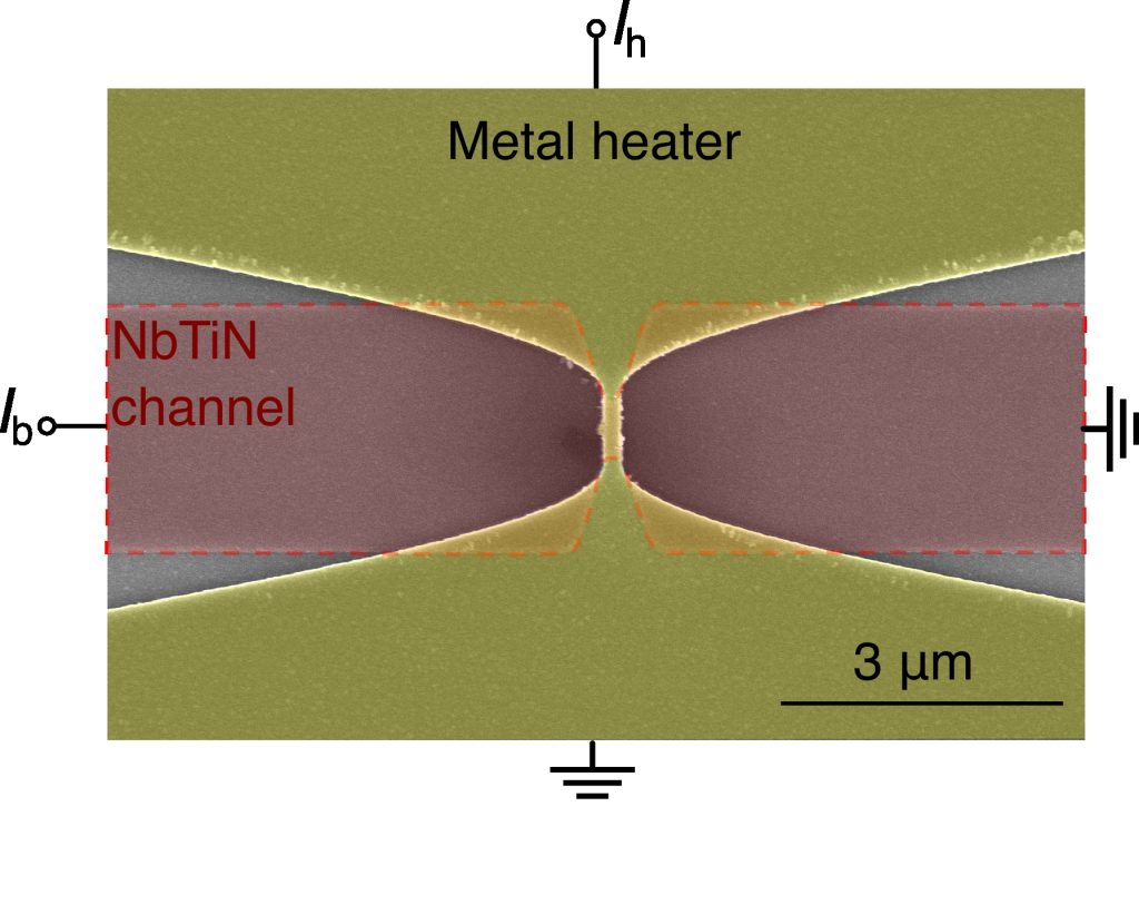
One of QUPSI’s primary research focuses is advancing data processing at cryogenic temperatures. As part of the European RESPITE project, our goal is to integrate vision and cognition onto a single chip capable of real-time image processing. Superconducting nanowire single-photon detectors (SNSPDs) are used to capture images at cryogenic temperatures, and our focus is on combining superconducting electronics and photonic technologies to process these images on the same chip. A key innovation in this work is the use of superconducting Joule switches (SJS). At QUPSI, we are involved in the full cycle of designing, fabricating, and testing these SJS in cleanroom and cryogenic setups, evaluating their performance in terms of power consumption, switching speed, and scalability. This architecture aims to evolve into an efficient, scalable neural network. The ongoing development of this technology will push the limits of cryogenic computing, opening the door to a new generation of neuromorphic systems.
Novel SNSPD fabrication methods and materials
Superconducting nanowire single-photon detectors (SNSPDs) are amongst the best contemporary light detection methods and their applications are ever increasing. Therefore investigating new materials, platforms and methods and for instance integration with other superconducting devices is potentially of great interest. In collaboration with Ali lab (Department of Quantum Nanoscience) we are investigating novel 2d materials as new SNSPD platforms. For these materials, entirely new fabrication methodologies have to be developed.
SNSPD Applications
3rd transparency window for neuroimaging
Our research focuses on developing advanced superconducting nanowire single-photon detectors (SNSPDs) for applications in neuroimaging and other high-resolution imaging fields. Our SNSPDs were instrumental in the groundbreaking work published in Nature Nanotechnology, where they enabled in vivo, non-invasive confocal fluorescence imaging beyond 1700 nm. This breakthrough opens new possibilities for precise biological imaging and is a key step towards advancing imaging technologies for brain and neural research.
FastMOT
In the EU-funded FastMOT project, we are developing an innovative fast-gated, ultra-high quantum efficiency superconducting nanowire single-photon detector (SNSPD) to enable multi-functional deep body imaging using diffuse optics. This technology will allow for the imaging of deep organs and monitoring of vital functions such as oxygenation levels, hemodynamics, perfusion, and metabolism. SNSPDs operate by transitioning from a superconducting to a resistive state upon detecting a single photon at cryogenic temperatures. They are highly sensitive across a broad wavelength range (UV to mid-infrared), with detection efficiencies over 90%. To address challenges related to cryogenic electronics integration and thermal limitations, we are developing a novel capacitive readout circuit using fast superconducting Joule switches. This innovation aims to simplify the SNSPD array design, enhancing its performance and scalability for advanced imaging applications.
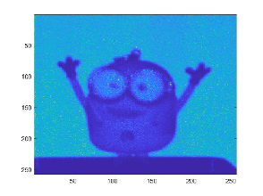
Lidar with SNSPDs
This is an ongoing project, as a teaser see below picture 🙂
Fourier spectroscopy with SNSPDs
Mid-infrared (MIR) spectrometers are vital for advancing fields such as molecular spectroscopy, atmospheric science, and chemical sensing due to their ability to probe fundamental vibrational transitions. Traditional detectors for MIR face limitations like low sensitivity and high noise. Superconducting detectors, such as SNSPDs, offer revolutionary advantages, including low noise, high sensitivity, and extended wavelength range. A MIR spectrometer that operates on low power is especially exciting as it enables applications in compact, energy-efficient setups, including cryostat environments or portable systems. This innovation bridges the gap between cutting-edge photonic detection and practical real-world applications in spectroscopy and beyond.
This is an on-going research – coming soon 🙂
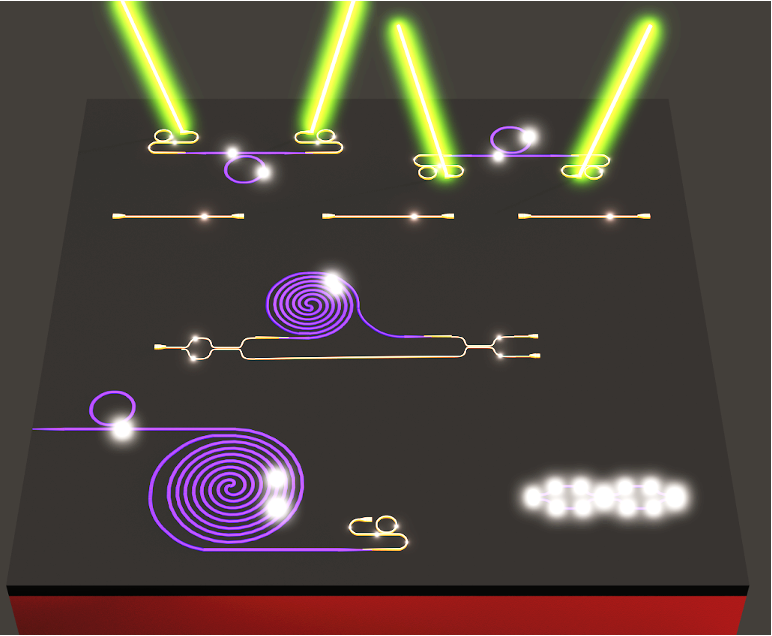
Integrated [quantum] Nanophotonics
In our Integrated Photonics team, we specialize in designing and fabricating integrated photonic devices across a range of material platforms, including amorphous silicon carbide, lithium niobate, silicon nitride, and silicon-on-insulator, for wavelengths spanning from the visible to the mid-infrared. A key area of focus is the deterministic integration of single-photon sources based on nanowires and superconducting single-photon detectors for quantum photonic experiments. By combining these materials on a single chip, we can leverage various optical effects. For example, integrating high-quality amorphous silicon carbide (known for strong third-order non-linearities) with lithium niobate (a second-order non-linear platform) enables heat-free, fast electro-optical modulation. This allows for the generation of entangled photon pairs, a key component for optical computing and quantum experiments. Another notable combination involves amorphous silicon carbide and silicon nitride, which provide high thermo-optic modulation and low-loss delay lines. Additionally, we’ve developed silicon dioxide claddings that allow precise tuning of thermo-optic properties on a single chip, enabling widely tunable and low-power integrated photonic circuits.
Integrated Photonics with amorphous silicon carbide
The goal is to design and fabricate high-performance integrated photonic devices using amorphous silicon carbide (a-SiC). Compared to its crystalline counterpart, amorphous silicon carbide is easier to integrate, offers greater flexibility with other material platforms, and exhibits higher third-order non-linearities, which are particularly useful for four-wave mixing. We have developed a deposition recipe for low-loss a-SiC at low temperatures, making it compatible with various material platforms and single-photon sources based on quantum dots. To tune the thermo-optic response of individual devices, we are deterministically depositing silicon dioxide to achieve positive, negative, and athermal wavelength shifts on a single chip. Our current goal is to integrate these advantages into a single chip, combining them with superconducting single-photon detectors for more complex applications, enabling low-power, widely tunable integrated photonic circuits.
Hybrid integration for reconfigurable photonics
By leveraging the strengths of various photonic integrated platforms, including silicon nitride, lithium niobate, and silicon carbide, we design, fabricate, and characterize hybrid photonic integrated circuits. These circuits encompass a wide range of effects, such as thermo-optics, electro-optics, and second and third-order nonlinearities, allowing us to benchmark fast and efficient reconfigurable photonic devices. A key milestone we aim to achieve is the integration of single-photon emitters and superconducting single-photon detectors on the same chip. Our ultimate goal is to create large-scale, low-loss, and efficiently tunable photonic circuits for applications in quantum photonics, optical computing, sensing, and imaging.